COXEM TABLETOP & COMPACT SEM-EDX

Excellent Resolution & Impressive Features at an Attractive Price

Tabletop SEM EM-30N

Tabletop SEM with Highest Resolution

Coxem-EM-30-Plus

Specifications

  • Highest resolution 5 nm (optical)
  • Tungsten or CeB6 filament
  • Variable high voltage 1-30 kV
  • SE- and BE-detector
  • Magnification up to 150,000x
  • XYT-stage motorized 35 mm x 35 mm x 45°
  • Z-Stage manual 45mm
  • Largest sample ∅ 70 mm
  • EDX detector (Oxford, Bruker)
  • Low Vacuum Mode
  • Joystick
  • CCD camera
  • Panorama module
  • Additional port for STEM, Cooling Stage or EBSD
  • Image size up to 5120 x 3840 px (TIF, BMP, PNG, JPG)

Tabletop SEM EM-30

Tabletop SEM at Lowest Price

Coxem-EM-30

Specifications

  • Highest resolution 5 nm (optical)
  • Tungsten filament
  • Variable high voltage 1-30 kV
  • SE detector
  • Magnification up to 150,000x
  • XYT-stage motorized 35 mm x 35 mm x 45°
  • Z-Stage manual 45mm
  • Largest sample ∅ 70 mm
  • EDX detector (Oxford, Bruker)
  • Image size up to 5120 x 3840 px (TIF, BMP, PNG, JPG)

Compact SEM CX-200 Plus

Compact SEM for Large Samples

Coxem-SEM-EDX-CX-200

Specifications

  • Highest resolution 3 nm (optical)
  • Tungsten filament
  • Variable high voltage 1-30 kV
  • SE- and BE-detector
  • Magnification up to 300,000x
  • XYT stage motorized 60 mm x 60 mm x 90°
  • Z-Stage motorized 55 mm
  • Largest sample ∅ 160 mm
  • EDX detector (Oxford, Bruker)
  • Low Vacuum Mode
  • Live camera
  • Panorama module
  • Additional ports for EBSD, STEM, Cooling Stage, etc.
  • Image size up to 5120 x 3840 px (TIF, BMP, PNG, JPG)

Small Picture Gallery

Coxem is a young and innovative manufacturer of compact high-resolution SEM-EDX instruments from Korea. The instruments convince with outstanding resolution and features that are otherwise only offered in large laboratory equipment. Above that the equipment comes for an attractive price.

The Coxem technology is now available in Germany and exclusively distributed by RJL Micro & Analytic.

Technology

Highest Resolution and Contrast

SE-BSE

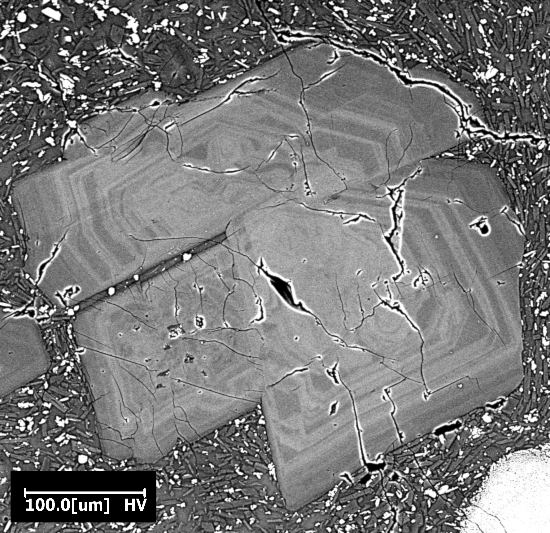
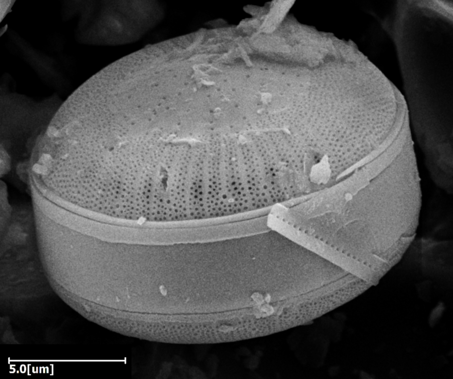
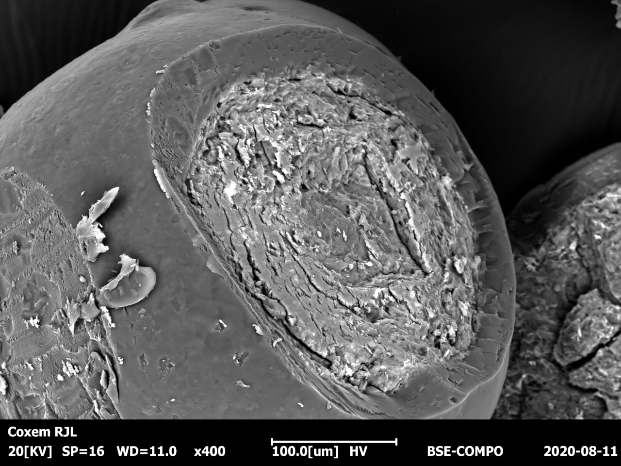
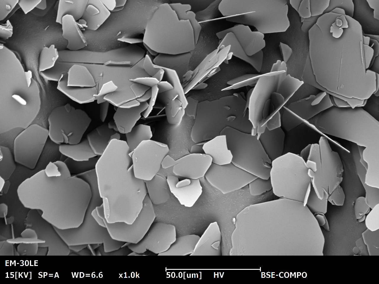
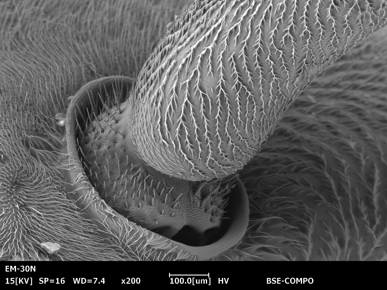
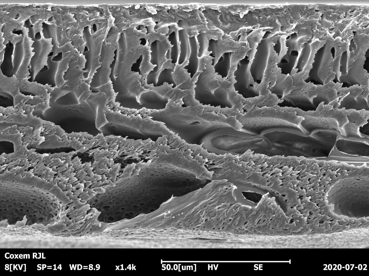
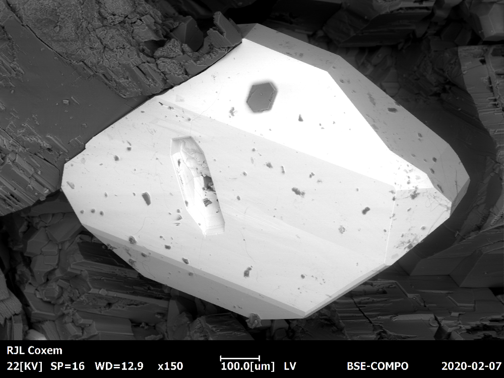
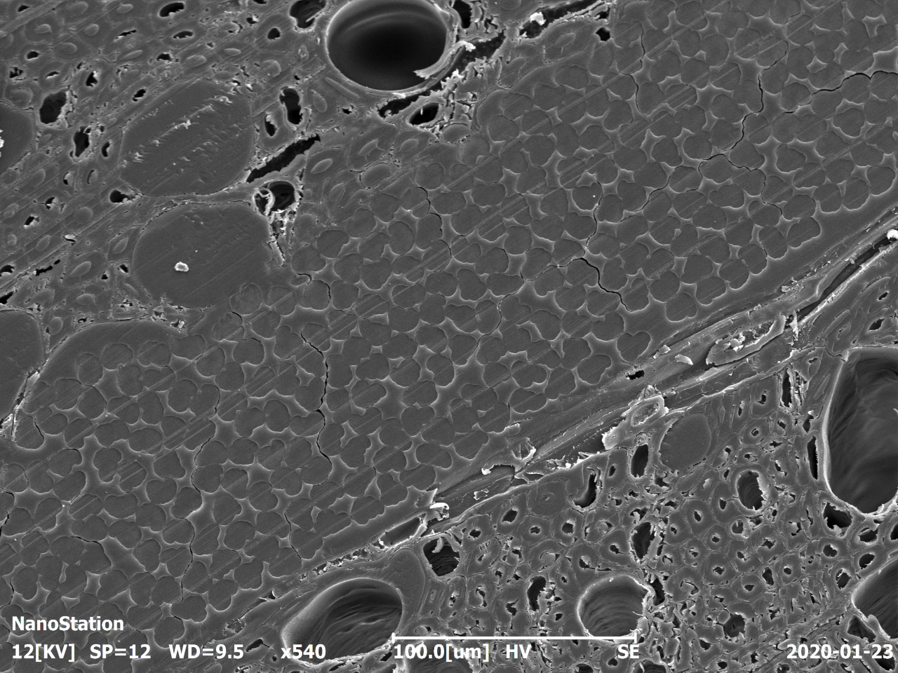
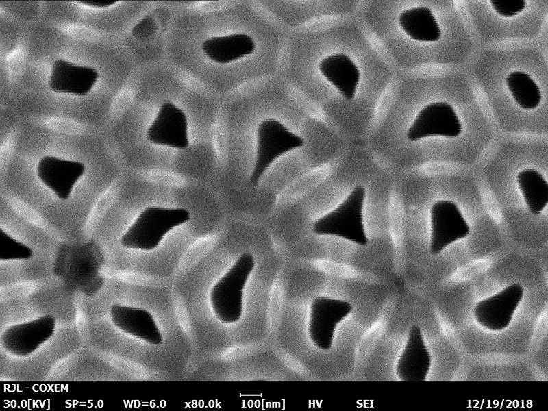
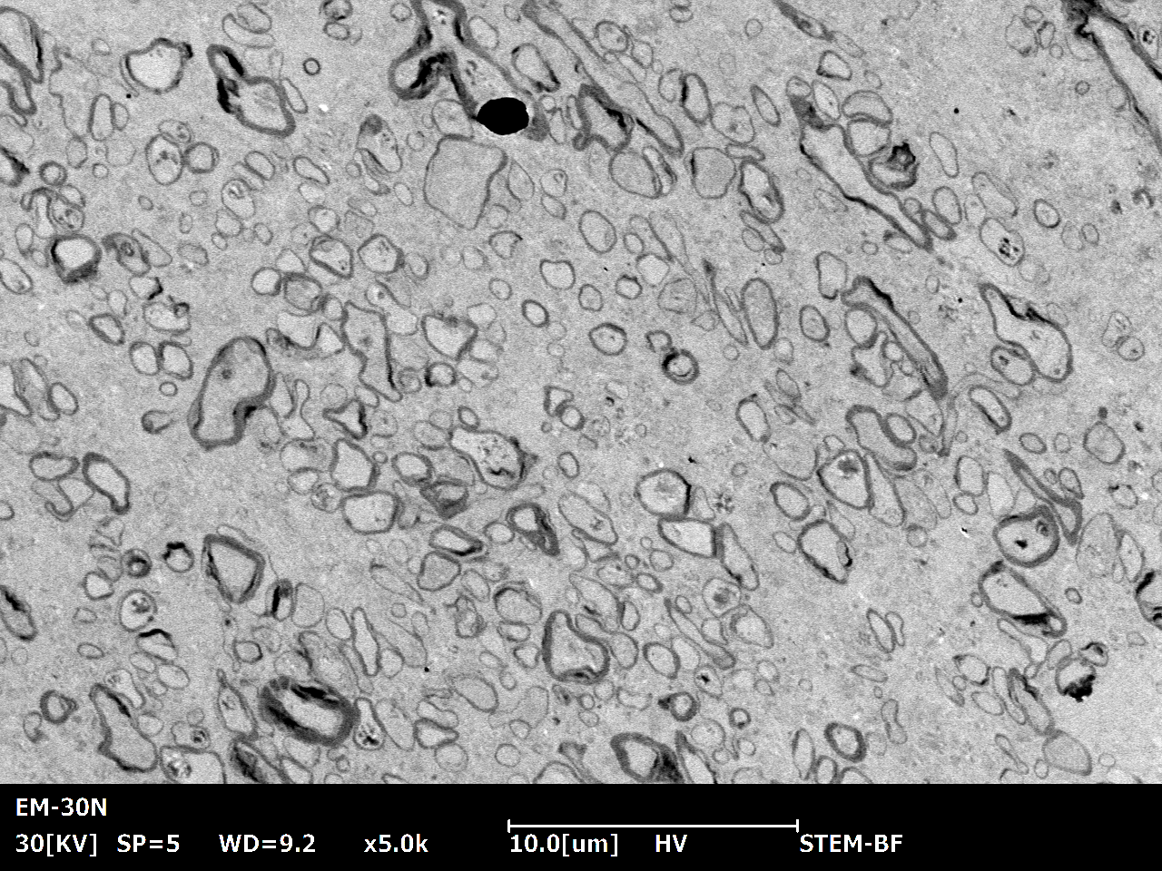
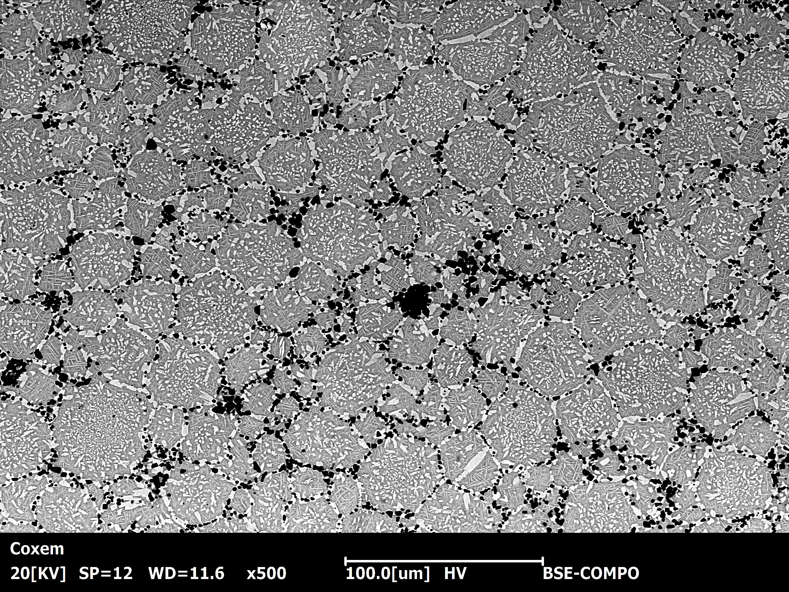
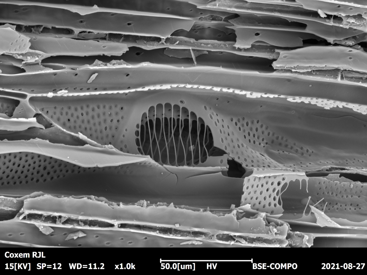
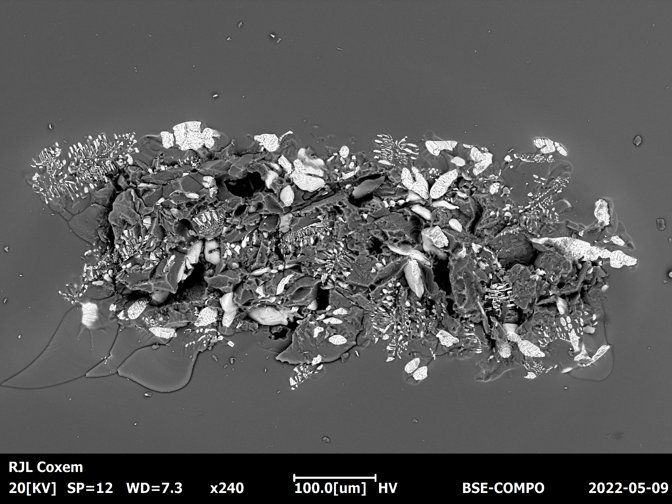
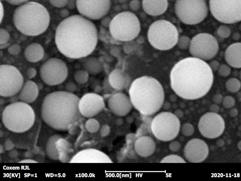
The newly developed electron optics of the Coxem compact SEMs achieve pin-sharp images at 100.000x magnification (left) and visualize the finest material contrast Z < 0.1 (right).

Variable High Voltage

Coxem-SEM-EDX-high-voltage

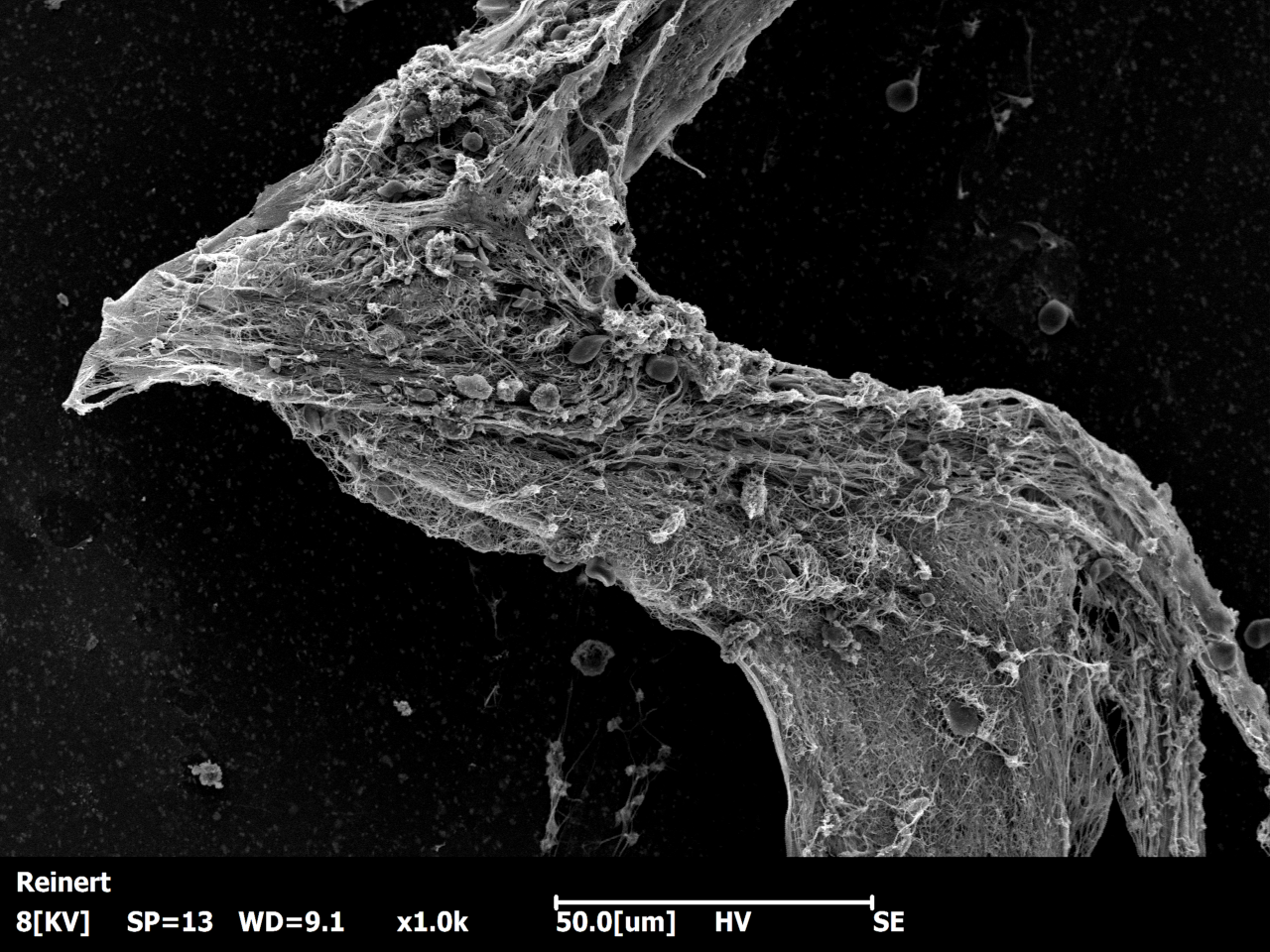
Even the finest surface structures can be visualized using a low acceleration voltage (high voltage 1-30 kV).

Low Vacuum Mode

Coxem-SEM-EDX-variable-pressure

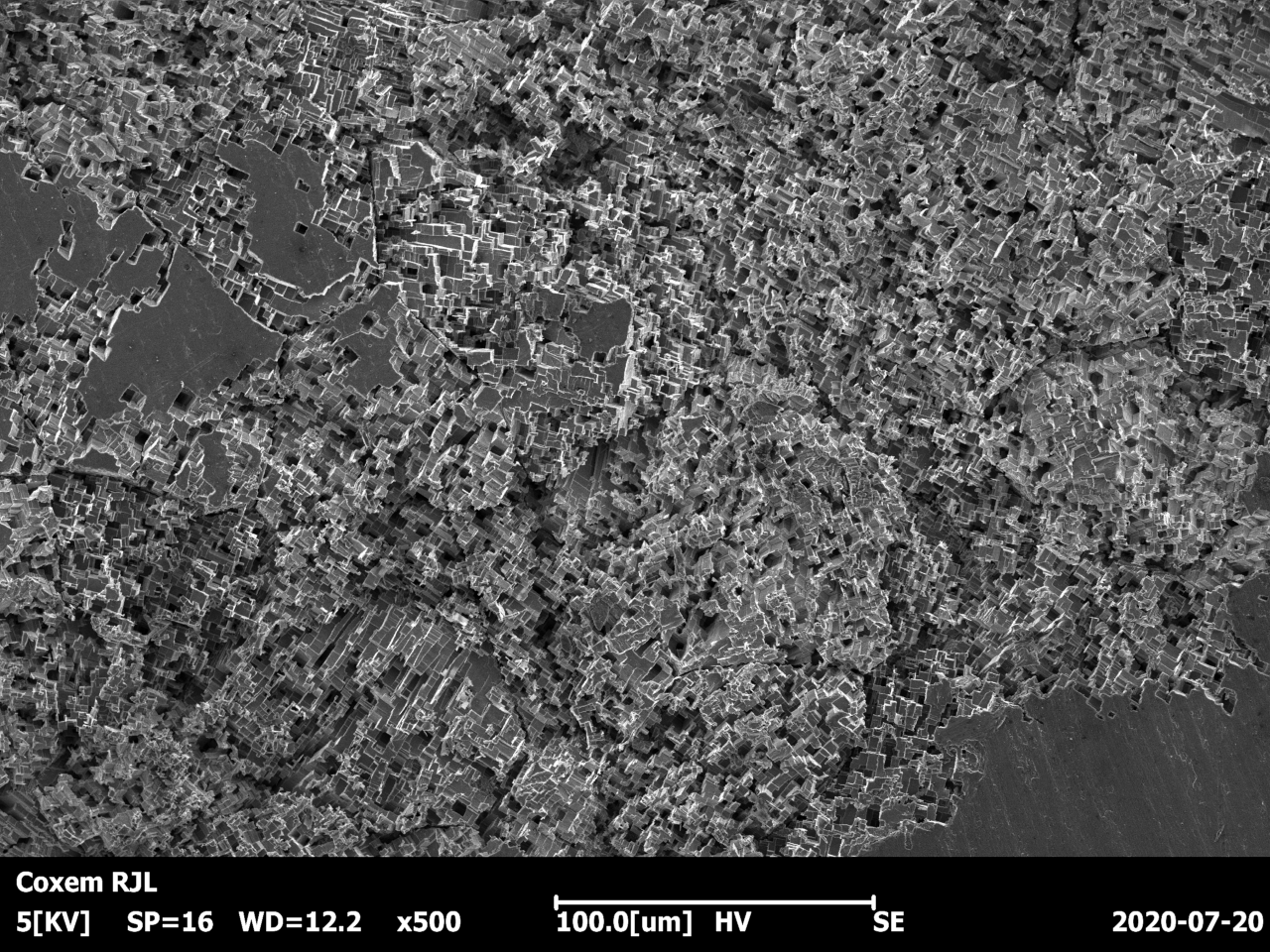
Residual air molecules of the low vacuum allow insulating samples to be discharged and microscopically examined (pressure 1-100 Pa).

You have the Choice

In addition to the classic tungsten technology, Coxem also offers beam generation using CeB6 filaments. Tungsten cathodes are widespread and very mature. The filaments can be exchanged by the user himself in a few simple steps. CeB6 filaments offer longer life and higher beam intensity, which can be an advantage when imaging with low voltage. However, the filaments are much more expensive and usually cannot be replaced by the user. Due to the different requirements for the operating vacuum level, CeB6 instruments must run in stand-by at all times. Tungsten instruments, on the other hand, can be switched off completely when not in use and are still operational within a few minutes.

User-Friendly Operation

Intuitive Control

Magnification, focus and XY-navigation can be operated using a 3D multifunction joystick

Coxem-Joystick

Simple Navigation

Color camera above stage, sample navigation by clicking

Coxem-Navigation-Camera

Wide Format Scan

Automatic imaging of large sample areas by stitching of single images (high-resolution mosaic)

Material & Element Analysis

Oxford AZtecOne EDX

XploreCompact X-ray element spectrometer, thermoelectrically cooled silicone drift detector (SDD), resolution 129 eV at Mn (K), sensitive from Z = 5 (boron), including AZtecOne software package

Oxford-EDX

Bruker Quantax EDX

XFlash 6 X-Ray element spectrometer, thermoelectrically cooled silicone drift detector (SDD), resolution 129 eV at Mn (K), sensitive from Z = 5 (boron), including Esprit Compact software package

Bruker-EDX

Bruker Quantax XS

eFlash XS detector for electron backscatter diffraction (EBSD), no calibration required, available in combination with EDX, including Esprit software package

EBSD-2

Equipment

In-Situ Sample Cooling

Peltier sample cooling down to -25°C for microscopic imaging of biological and liquid preparations in a vacuum

Coxem SEM-EDX Cooling stage

STEM module

Module for scanning transmission microscopy (STEM), BF and DF sensor, including holder for up to four TEM networks

STEM-

Conductive Coating

Sputter for Au, Pt and other targets, ionization current variable 0-9 mA

Coxem-Sputter

Vibration Protection

Anti-vibration table for SEM-EDX instrument (active)

Antivibration

Cross-Section Polisher

Preparation tool for the production of high-precision cross-sections for SEM-EDX, EBSD, surface polishing by argon ion beam