PARTICLES
PROBLEM?
REMAINING DIRT ANALYSIS
ROENTGEN
HIGH RESOLUTION
3D X-RAY MICROSCOPY
WHAT? HOW MUCH
AND FROM WHERE?
EDX ELEMENTAL ANALYSIS
QUICK TEST
CLEANLINESS
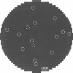
VDA-19 PARTICLE SCANNER
QUALITY
TESTED
ACCREDITED ANALYZES
FASCINATING
INSIGHTS
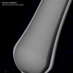
X-RAY MICRO/NANO-CT
REMAINING DIRT
ANALYZE
TECHNICAL CLEANLINESS
TABLETS
UNDERSTAND
3D MICROTOMOGRAPHY
MATERIAL & STRUCTURE
ANALYTICS
CONSULT A TEST LABORATORY
NON-DESTRUCTIVE
TEST
PORE ANALYSIS IN 3D
DAMAGE
HARD PARTICLES
DETERMINE PARTICLE HARDNESS
SPECTRAL
PICTURES
RAMAN MICROSCOPY
INSIGHT
PLEASE?
3D TAXONOMY VIRTUAL
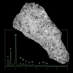
Microscopic examination & elemental analysis in one step
SEM-EDX
Operating Principle
In scanning electron microscopy (SEM), a focused primary electron beam is rastered stepwise across the sample. At each pixel, the reflected electrons are detected, yielding a microscopic greyscale image of the sample. There are two imaging techniques:
Backscattered electrons (BE) → material contrast
Secondary electrons (SE) → topography contrast
In addition, the primary electron beam triggers the sample to emit characteristic X-Rays. The elements in the sample as well as their respective modal weights can be precisely determined by analyzing the color spectrum in an EDX detector.
Applications
Examination of damage and wear on a microscopic level
Analysis of aging, corrosion and oxidation of components
Determination of the origin of the particles, chips and particles that lead to failure
Error analysis in the delamination of coatings and paints
Investigation of electrical contact problems
Analysis of surfaces and coatings
Material determination and microstructural analysis