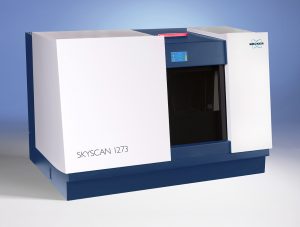


We recently supported Bruker Nano in installing a compact EBSD system for the first time in the world on our Coxem Tabletop SEM-EDX Thanks to good preparation, the installation went smoothly and after an hour we were able to record the first EBSD mappings. For Bruker and Coxem, this test represents an important step towards commercializing EBSD technology for SEM-EDX desktop devices.

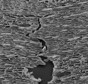
Electron Backscatter Diffraction (EBSD) provides line patterns (so-called Kikuchi patterns) that reflect the crystallographic orientation of the examined sample areas. Commercially available aluminum foil was used as the test object and an area of approx. 40 µm x 80 µm was measured over a period of one hour.

We were particularly impressed by the stability of the electron beam during the entire acquisition period, which is not necessarily given for larger SEMs. We were able to collect promising results on this comparatively complicated sample, which confirm the feasibility of the EBSD applications in the compact table format.
-
- Semi-automatic grain size and shape distribution analysis
- Quantitative analysis of microstructures and sub-areas
- Determination of the area or volume fraction of deformed or recrystallized grains
- Grain boundary analysis
- Phase identification and phase distribution analysis
- Correlation of chemical and crystallographic results
- Orientation distribution analysis - crystallographic texture analysis
-
- SE – Secondary electron microscopy for imaging by topography and morphology
- BSE – Backscattered electron icroscopy for imaging by material contrast
- EDX – X-ray element spectroscopy
- STEM - Transmission electron microscopy
- ESBD - Electron backscatter diffraction for crystallographic orientation
- Sputter - Sample coating for conductivity
- Cooling Stage - Sample cooling for vacuum-unstable samples
- Low vacuum - Discharge of non-conductive materials
- Cross-Section Polisher - Surface polishing