SEM-EDX GUIDE FOR BUYERS

Chapter 3 - Imaging and Spectroscopy Detectors

Standard Types of Detector

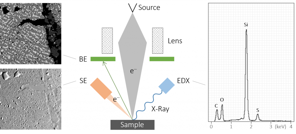
During operation of the SEM, the electron beam is scanned point by point over the sample. The backscattered electrons are counted in the imaging detectors. At the same time, the electron beam excites the sample to emit characteristic X-rays. By analyzing the X-ray spectrum, the elements in the sample can be determined. Three detector systems are considered standard for SEM devices:

  • Backscattered electrons (BE) → material contrast
  • Secondary electrons (SE) → topography contrast
  • Energy dispersive X-ray spectroscopy (EDX) → elemental analysis
 

The following diagram shows the generation of the primary electron beam, its interaction with the sample and the arrangement of the detector systems:

Backscatter and Secondary Electrons (BE / SE)

For imaging, backscatter and secondary electron detectors have prevailed. The backscattered electrons (BE) show the element or material contrast of the sample. The heavier an element is, the brighter the area in the BE image appears. The secondary electrons (SE) originate from the surface and reflect the topography of the sample.

Note that the SEM device of your choice can integrate both BE and SE detector systems. The information content is complementary and in the practical work the consideration of both modalities is essential.

X-Ray Element Analysis (EDX)

Elemental analysis using X-ray spectroscopy (EDX) is optionally available on all SEM devices. Some manufacturers offer their own hardware and software, while others integrate EDX systems from specialized third-party suppliers. Their software is much further developed, offers maximum functionality including quantitative analysis and can be retrospectively expanded. If required, additional software modules (eg for automatic particle analysis) can be activated.

Here's to check if the simplified features of SEM manufacturers offering their own EDX solutions will not affect your future expansion possibilities.

Transmission Electrons (STEM)

Recently, Scanning Transmission Electron Microscopy (STEM) is no longer reserved for large research equipment only. Some tabletop SEMs and compact devices with STEM detectors offer the possibility to image thin sections on standardized TEM grids. In particular, for organic preparations and tissue sections, this novel option is interesting because an energy of 30 kV is already sufficient to irradiate such thin sections.